TOP100YN Power Integrations IC OFFLINE SWIT PWM OTP HV TO220
Integraallülitused (IC-d)
Tootja number:
TOP100YN
Tootja:
Tootekategooria:
Kirjeldus:
IC OFFLINE SWIT PWM OTP HV TO220
RoHs olek:
Andmetabelid:
Juhtimisfunktsioonid :
-
Osa olek :
Obsolete
Paigaldustüüp :
Through Hole
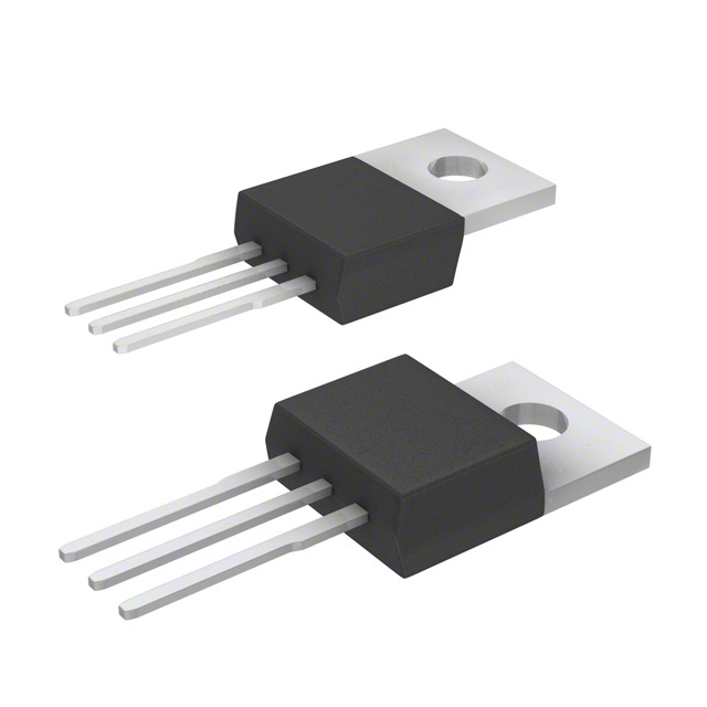
Pakend/ümbris :
TO-220-3
Pakendamine :
Tube
Pinge – käivitamine :
-
Pinge – rike :
350V
Pinge – toide (Vcc/Vdd) :
-
Sagedus – ümberlülitamine :
100kHz
seeria :
TOPSwitch®
Sisemised lülitid :
Yes
Tarnija seadmepakett :
TO-220-3
Töötemperatuur :
-40°C ~ 150°C (TJ)
Töötsükkel :
67%
Väljundi isoleerimine :
Isolated
Veakaitse :
Current Limiting, Over Temperature
Võimsus (vatti) :
30W
Topoloogia :
Boost, Buck, Flyback, Forward
Laos
31,067
Ühiku hind:
Võtke meiega ühendust Pakkumine
TOP100YN Konkurentsivõimelised hinnad
ChipIcil on ainulaadne tarneallikas. Pakume oma klientidele TOP100YN konkurentsivõimelise hinnaga. Saate nautida meie parimat teenust, ostes ChipIc TOP100YN. Parima hinna saamiseks saidil TOP100YN võtke meiega ühendust.
Hinnapakkumise saamiseks klõpsake
TOP100YN Iseärasused
TOP100YN is produced by Power Integrations, belongs to DC-DC muundurid PMIC - AC, eraldiseisvad lülitid.
TOP100YN Toote üksikasjad
:
TOP100YN – DC-DC muundurid PMIC - AC, eraldiseisvad lülitid disainitud puhvervõimendid ja toodetud Power Integrations.
TOP100YN, mida pakub Power Integrations, saab osta CHIPMLCC-st.
Siit leiate erinevaid juhtivate tootjate elektroonilisi osi rahu.
CHIPMLCC TOP100YN on range kvaliteedikontrolliga ja nõuetele vastav kõike nõuetele.
CHIPMLCC-s näidatud fondi staatus on ainult viitamiseks.
Kui te ei leia otsitavat osa, võtke meiega ühendust lisateavet, näiteks varude arvu andmetabelis TOP100YN (PDF), hind TOP100YN, Pinout TOP100YN, manuaal TOP100YN Ja TOP100YN asenduslahendus.
TOP100YN FAQ
:
1. What is the difference between NPN and PNP transistors?
NPN and PNP transistors are both bipolar junction transistors, but they have opposite polarities. In an NPN transistor, current flows from the collector to the emitter when a small current is applied to the base, while in a PNP transistor, current flows from the emitter to the collector when a small current is applied to the base.
2. How does a diode work?
A diode is a semiconductor device that allows current to flow in only one direction. When a positive voltage is applied to the anode and a negative voltage to the cathode, the diode conducts and allows current to flow. When the polarity is reversed, the diode blocks the current flow.
3. What is the function of a voltage regulator?
A voltage regulator is used to maintain a constant output voltage in a circuit, regardless of changes in input voltage or load conditions. It ensures that the voltage supplied to the load remains within specified limits, providing stable and reliable operation.
4. What are the key differences between analog and digital circuits?
Analog circuits process continuous signals, while digital circuits process discrete signals represented by binary digits (0s and 1s). Analog circuits are sensitive to noise and require precise component values, whereas digital circuits are more immune to noise and can perform logical operations.
5. How does a MOSFET differ from a BJT?
MOSFETs (Metal-Oxide-Semiconductor Field-Effect Transistors) are voltage-controlled devices, while BJTs (Bipolar Junction Transistors) are current-controlled devices. MOSFETs have high input impedance and are suitable for high-frequency applications, whereas BJTs have low input impedance and are commonly used in low-frequency amplification.
6. What is the purpose of a Schottky diode?
A Schottky diode is known for its fast switching speed and low forward voltage drop. It is commonly used in high-frequency and high-speed applications, such as rectification, clamping, and RF detection.
7. How do you calculate the power dissipation in a semiconductor device?
The power dissipation in a semiconductor device can be calculated using the formula P = I^2 * R, where P is the power dissipation, I is the current flowing through the device, and R is the resistance of the device. Additionally, the power dissipation can be affected by the ambient temperature and thermal resistance of the device.
8. What is the significance of the bandgap energy in semiconductors?
The bandgap energy determines the electrical conductivity of a semiconductor material. A larger bandgap results in lower conductivity, making the material suitable for insulating or high-temperature applications. Conversely, a smaller bandgap leads to higher conductivity, making the material suitable for electronic and optoelectronic devices.
9. How does doping affect the behavior of a semiconductor?
Doping introduces impurities into a semiconductor to modify its electrical properties. N-type doping adds electrons to the semiconductor, increasing its conductivity, while P-type doping creates "holes" in the crystal lattice, leading to decreased conductivity. Doping is essential for creating p-n junctions and controlling the behavior of semiconductor devices.
10. What are the advantages of using gallium nitride (GaN) in power electronics?
Gallium nitride offers several advantages over traditional silicon-based power devices, including higher breakdown voltage, lower on-resistance, and faster switching speeds. These characteristics make GaN devices well-suited for high-efficiency power conversion applications, such as in electric vehicles, renewable energy systems, and telecommunications infrastructure.
TOP100YN Seotud märksõnad
:
TOP100YN Hind
TOP100YN Maalimine
TOP100YN Tihvtide pinge
Pakkumised: Kiire hinnapakkumise kontroll
Minimaalne tellimus: 1
Sisaldab "TOP1" seeria tooteid