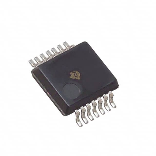
SN74LVC574ADWR Texas Instruments IC FF D-TYPE SNGL 8BIT 20SOIC
Integraallülitused (IC-d)
Tootja number:
SN74LVC574ADWR
Tootja:
Tootekategooria:
Kirjeldus:
IC FF D-TYPE SNGL 8BIT 20SOIC
RoHs olek:
Andmetabelid:
Elementide arv :
1
Funktsioon :
Standard
Kella sagedus :
150MHz
Maksimaalne levimisviivitus @ V, Max CL :
6.8ns @ 3.3V, 50pF
Osa olek :
Active
Päästiku tüüp :
Positive Edge
Paigaldustüüp :
Surface Mount
Pakend/ümbris :
20-SOIC (0.295", 7.50mm Width)
Pakendamine :
Tape & Reel (TR)
Pinge – toide :
1.65 V ~ 3.6 V
Praegune – vaikne (Iq) :
1.5µA
seeria :
74LVC
Sisendvõimsus :
4pF
Töötemperatuur :
-40°C ~ 125°C (TA)
Tüüp :
D-Type
Väljundi tüüp :
Tri-State, Non-Inverted
Vool – väljund kõrge, madal :
24mA, 24mA
Bittide arv elemendi kohta :
8
Laos
22,995
Ühiku hind:
Võtke meiega ühendust Pakkumine
SN74LVC574ADWR Konkurentsivõimelised hinnad
ChipIcil on ainulaadne tarneallikas. Pakume oma klientidele SN74LVC574ADWR konkurentsivõimelise hinnaga. Saate nautida meie parimat teenust, ostes ChipIc SN74LVC574ADWR. Parima hinna saamiseks saidil SN74LVC574ADWR võtke meiega ühendust.
Hinnapakkumise saamiseks klõpsake
SN74LVC574ADWR Iseärasused
SN74LVC574ADWR is produced by Texas Instruments, belongs to Loogika – Flip Flops.
SN74LVC574ADWR Toote üksikasjad
:
SN74LVC574ADWR – Loogika – Flip Flops disainitud puhvervõimendid ja toodetud Texas Instruments.
SN74LVC574ADWR, mida pakub Texas Instruments, saab osta CHIPMLCC-st.
Siit leiate erinevaid juhtivate tootjate elektroonilisi osi rahu.
CHIPMLCC SN74LVC574ADWR on range kvaliteedikontrolliga ja nõuetele vastav kõike nõuetele.
CHIPMLCC-s näidatud fondi staatus on ainult viitamiseks.
Kui te ei leia otsitavat osa, võtke meiega ühendust lisateavet, näiteks varude arvu andmetabelis SN74LVC574ADWR (PDF), hind SN74LVC574ADWR, Pinout SN74LVC574ADWR, manuaal SN74LVC574ADWR Ja SN74LVC574ADWR asenduslahendus.
SN74LVC574ADWR FAQ
:
1. What is the operating voltage range for the SN74LVC574ADWR?
The operating voltage range for the SN74LVC574ADWR is 2 V to 3.6 V.
2. What is the maximum input clamp current for this device?
The maximum input clamp current for the SN74LVC574ADWR is ±20 mA.
3. Can this device be used in a daisy-chain configuration?
Yes, the SN74LVC574ADWR can be used in a daisy-chain configuration for serial data transfer.
4. What is the typical output rise/fall time for this latch?
The typical output rise/fall time for the SN74LVC574ADWR is 0.8 ns.
5. Is the SN74LVC574ADWR compatible with 5V TTL/CMOS logic levels?
Yes, this device is compatible with 5V TTL/CMOS logic levels when used with appropriate level-shifting techniques.
6. What is the maximum propagation delay for the SN74LVC574ADWR?
The maximum propagation delay for this latch is 5.3 ns.
7. Can the SN74LVC574ADWR withstand electrostatic discharge (ESD)?
Yes, this device has ESD protection and can withstand up to 2000 V human-body model (HBM) ESD.
8. What is the maximum quiescent current consumption of the SN74LVC574ADWR?
The maximum quiescent current consumption of this latch is 10 µA at 25°C.
9. Does the SN74LVC574ADWR have an integrated output diode for inductive load protection?
No, this device does not have an integrated output diode for inductive load protection.
10. What is the package type and dimensions for the SN74LVC574ADWR?
The SN74LVC574ADWR is available in a SOIC-20 package with dimensions of 12.8 mm x 7.5 mm.
SN74LVC574ADWR Seotud märksõnad
:
SN74LVC574ADWR Hind
SN74LVC574ADWR Maalimine
SN74LVC574ADWR Tihvtide pinge
Pakkumised: Kiire hinnapakkumise kontroll
Minimaalne tellimus: 1
Sisaldab "SN74" seeria tooteid