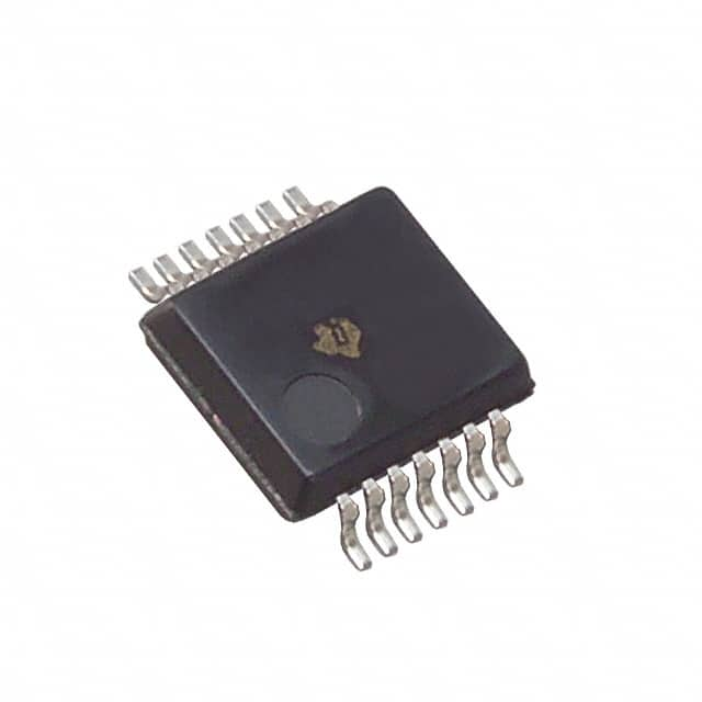
SN74LS259BN Texas Instruments IC 8-BIT ADDRESSBLE LATCH 16-DIP
Integraallülitused (IC-d)
Tootja number:
SN74LS259BN
Tootja:
Tootekategooria:
Kirjeldus:
IC 8-BIT ADDRESSBLE LATCH 16-DIP
RoHs olek:
Andmetabelid:
Ahel :
1:8
Loogika tüüp :
D-Type, Addressable
Osa olek :
Active
Paigaldustüüp :
Through Hole
Pakend/ümbris :
16-DIP (0.300", 7.62mm)
Pakendamine :
Tube
Pinge – toide :
4.75 V ~ 5.25 V
seeria :
74LS
Sõltumatud vooluringid :
1
Tarnija seadmepakett :
16-PDIP
Töötemperatuur :
0°C ~ 70°C
Väljundi tüüp :
Standard
Viivitusaeg – levik :
19ns
Vool – väljund kõrge, madal :
400µA, 8mA
Laos
49,945
Ühiku hind:
Võtke meiega ühendust Pakkumine
SN74LS259BN Konkurentsivõimelised hinnad
ChipIcil on ainulaadne tarneallikas. Pakume oma klientidele SN74LS259BN konkurentsivõimelise hinnaga. Saate nautida meie parimat teenust, ostes ChipIc SN74LS259BN. Parima hinna saamiseks saidil SN74LS259BN võtke meiega ühendust.
Hinnapakkumise saamiseks klõpsake
SN74LS259BN Iseärasused
SN74LS259BN is produced by Texas Instruments, belongs to Loogika – riivid.
SN74LS259BN Toote üksikasjad
:
SN74LS259BN – Loogika – riivid disainitud puhvervõimendid ja toodetud Texas Instruments.
SN74LS259BN, mida pakub Texas Instruments, saab osta CHIPMLCC-st.
Siit leiate erinevaid juhtivate tootjate elektroonilisi osi rahu.
CHIPMLCC SN74LS259BN on range kvaliteedikontrolliga ja nõuetele vastav kõike nõuetele.
CHIPMLCC-s näidatud fondi staatus on ainult viitamiseks.
Kui te ei leia otsitavat osa, võtke meiega ühendust lisateavet, näiteks varude arvu andmetabelis SN74LS259BN (PDF), hind SN74LS259BN, Pinout SN74LS259BN, manuaal SN74LS259BN Ja SN74LS259BN asenduslahendus.
SN74LS259BN FAQ
:
1. What is the function of the SN74LS259BN?
The SN74LS259BN is an 8-bit addressable latch designed for general-purpose storage applications in digital systems.
2. What is the operating voltage range of the SN74LS259BN?
The operating voltage range of the SN74LS259BN is 4.75V to 5.25V.
3. What is the maximum clock frequency supported by the SN74LS259BN?
The SN74LS259BN supports a maximum clock frequency of 33 MHz.
4. Can the SN74LS259BN be used in parallel operations?
Yes, the SN74LS259BN can be used in parallel operations to enable multiple devices to share the same data bus.
5. What is the typical power dissipation of the SN74LS259BN?
The typical power dissipation of the SN74LS259BN is 50mW.
6. Is the SN74LS259BN compatible with TTL logic levels?
Yes, the SN74LS259BN is compatible with TTL logic levels.
7. What is the package type of the SN74LS259BN?
The SN74LS259BN is available in a 16-pin DIP (Dual In-line Package).
8. Does the SN74LS259BN have internal latches for data storage?
Yes, the SN74LS259BN has internal latches for data storage, allowing it to retain information even when the clock signal is not active.
9. Can the SN74LS259BN be cascaded for expanded functionality?
Yes, the SN74LS259BN can be cascaded to create larger storage registers or addressable memory banks.
10. What are the typical applications of the SN74LS259BN?
The SN74LS259BN is commonly used in microprocessor systems, address decoding, and general digital storage applications.
SN74LS259BN Seotud märksõnad
:
SN74LS259BN Hind
SN74LS259BN Maalimine
SN74LS259BN Tihvtide pinge
Pakkumised: Kiire hinnapakkumise kontroll
Minimaalne tellimus: 1
Sisaldab "SN74" seeria tooteid