SN74LS257BDG4 Texas Instruments IC DATA SELECTOR/MUX SGL 16SOIC
Integraallülitused (IC-d)
Tootja number:
SN74LS257BDG4
Tootja:
Tootekategooria:
Kirjeldus:
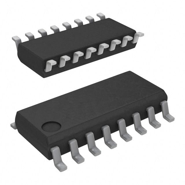
IC DATA SELECTOR/MUX SGL 16SOIC
RoHs olek:
Andmetabelid:
Ahel :
4 x 2:1
Osa olek :
Active
Paigaldustüüp :
Surface Mount
Pakend/ümbris :
16-SOIC (0.154", 3.90mm Width)
Pakendamine :
Tube
Pinge – toide :
4.75 V ~ 5.25 V
seeria :
74LS
Sõltumatud vooluringid :
1
Tarnija seadmepakett :
16-SOIC
Töötemperatuur :
0°C ~ 70°C
Tüüp :
Multiplexer
Vool – väljund kõrge, madal :
2.6mA, 24mA
Pinge toiteallikas :
Single Supply
Laos
43,818
Ühiku hind:
Võtke meiega ühendust Pakkumine
SN74LS257BDG4 Konkurentsivõimelised hinnad
ChipIcil on ainulaadne tarneallikas. Pakume oma klientidele SN74LS257BDG4 konkurentsivõimelise hinnaga. Saate nautida meie parimat teenust, ostes ChipIc SN74LS257BDG4. Parima hinna saamiseks saidil SN74LS257BDG4 võtke meiega ühendust.
Hinnapakkumise saamiseks klõpsake
SN74LS257BDG4 Iseärasused
SN74LS257BDG4 is produced by Texas Instruments, belongs to Loogika – signaali lülitid, multiplekserid, dekoodrid.
SN74LS257BDG4 Toote üksikasjad
:
SN74LS257BDG4 – Loogika – signaali lülitid, multiplekserid, dekoodrid disainitud puhvervõimendid ja toodetud Texas Instruments.
SN74LS257BDG4, mida pakub Texas Instruments, saab osta CHIPMLCC-st.
Siit leiate erinevaid juhtivate tootjate elektroonilisi osi rahu.
CHIPMLCC SN74LS257BDG4 on range kvaliteedikontrolliga ja nõuetele vastav kõike nõuetele.
CHIPMLCC-s näidatud fondi staatus on ainult viitamiseks.
Kui te ei leia otsitavat osa, võtke meiega ühendust lisateavet, näiteks varude arvu andmetabelis SN74LS257BDG4 (PDF), hind SN74LS257BDG4, Pinout SN74LS257BDG4, manuaal SN74LS257BDG4 Ja SN74LS257BDG4 asenduslahendus.
SN74LS257BDG4 FAQ
:
1. What is the operating voltage range for SN74LS257BDG4?
The operating voltage range for SN74LS257BDG4 is 4.75V to 5.25V.
2. What is the maximum input current for SN74LS257BDG4?
The maximum input current for SN74LS257BDG4 is ±20mA.
3. What is the typical propagation delay time for SN74LS257BDG4?
The typical propagation delay time for SN74LS257BDG4 is 15ns.
4. What is the maximum quiescent power consumption for SN74LS257BDG4?
The maximum quiescent power consumption for SN74LS257BDG4 is 16mW.
5. What is the maximum junction temperature for SN74LS257BDG4?
The maximum junction temperature for SN74LS257BDG4 is 150°C.
6. What is the package type for SN74LS257BDG4?
SN74LS257BDG4 comes in a SOIC-16 package.
7. What is the recommended operating temperature range for SN74LS257BDG4?
The recommended operating temperature range for SN74LS257BDG4 is 0°C to 70°C.
8. What is the output drive capability for SN74LS257BDG4?
The output drive capability for SN74LS257BDG4 is ±4mA.
9. What is the maximum input voltage for SN74LS257BDG4?
The maximum input voltage for SN74LS257BDG4 is 7V.
10. What is the pin configuration for SN74LS257BDG4?
Pin 1: GND, Pin 8: VCC, Pin 9: A0, Pin 10: A1, Pin 11: A2, Pin 12: A3, Pin 13: Y3, Pin 14: Y2, Pin 15: Y1, Pin 16: Y0.
SN74LS257BDG4 Seotud märksõnad
:
SN74LS257BDG4 Hind
SN74LS257BDG4 Maalimine
SN74LS257BDG4 Tihvtide pinge
Pakkumised: Kiire hinnapakkumise kontroll
Minimaalne tellimus: 1
Sisaldab "SN74" seeria tooteid