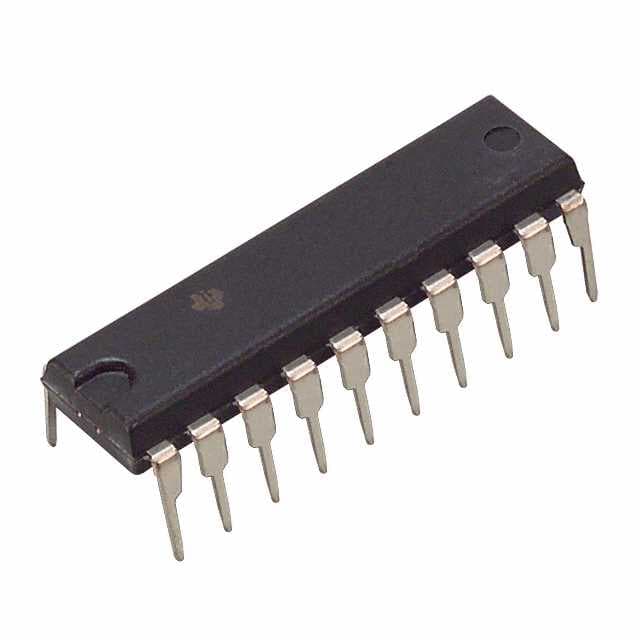
SN74ABT541BN Texas Instruments IC BUF NON-INVERT 5.5V 20PDIP
Integraallülitused (IC-d)
Tootja number:
SN74ABT541BN
Tootja:
Tootekategooria:
Kirjeldus:
IC BUF NON-INVERT 5.5V 20PDIP
RoHs olek:
Andmetabelid:
Elementide arv :
1
Loogika tüüp :
Buffer, Non-Inverting
Osa olek :
Active
Paigaldustüüp :
Through Hole
Pakend/ümbris :
20-DIP (0.300", 7.62mm)
Pakendamine :
Tube
Pinge – toide :
4.5 V ~ 5.5 V
seeria :
74ABT
Sisendtüüp :
-
Tarnija seadmepakett :
20-PDIP
Töötemperatuur :
-40°C ~ 85°C (TA)
Väljundi tüüp :
Push-Pull
Vool – väljund kõrge, madal :
32mA, 64mA
Bittide arv elemendi kohta :
8
Laos
20,740
Ühiku hind:
Võtke meiega ühendust Pakkumine
SN74ABT541BN Konkurentsivõimelised hinnad
ChipIcil on ainulaadne tarneallikas. Pakume oma klientidele SN74ABT541BN konkurentsivõimelise hinnaga. Saate nautida meie parimat teenust, ostes ChipIc SN74ABT541BN. Parima hinna saamiseks saidil SN74ABT541BN võtke meiega ühendust.
Hinnapakkumise saamiseks klõpsake
SN74ABT541BN Iseärasused
SN74ABT541BN is produced by Texas Instruments, belongs to Loogika – puhvrid, draiverid, vastuvõtjad, transiiverid.
SN74ABT541BN Toote üksikasjad
:
SN74ABT541BN – Loogika – puhvrid, draiverid, vastuvõtjad, transiiverid disainitud puhvervõimendid ja toodetud Texas Instruments.
SN74ABT541BN, mida pakub Texas Instruments, saab osta CHIPMLCC-st.
Siit leiate erinevaid juhtivate tootjate elektroonilisi osi rahu.
CHIPMLCC SN74ABT541BN on range kvaliteedikontrolliga ja nõuetele vastav kõike nõuetele.
CHIPMLCC-s näidatud fondi staatus on ainult viitamiseks.
Kui te ei leia otsitavat osa, võtke meiega ühendust lisateavet, näiteks varude arvu andmetabelis SN74ABT541BN (PDF), hind SN74ABT541BN, Pinout SN74ABT541BN, manuaal SN74ABT541BN Ja SN74ABT541BN asenduslahendus.
SN74ABT541BN FAQ
:
1. What is the maximum operating voltage for the SN74ABT541BN?
The maximum operating voltage for the SN74ABT541BN is 5.5V.
2. What is the typical input high-level voltage for this semiconductor?
The typical input high-level voltage for the SN74ABT541BN is 2V.
3. Can you provide the maximum propagation delay time for this device?
The maximum propagation delay time for the SN74ABT541BN is 6.5ns.
4. What is the output drive capability of the SN74ABT541BN?
The output drive capability of the SN74ABT541BN is ±32mA.
5. Is the SN74ABT541BN compatible with both CMOS and TTL input levels?
Yes, the SN74ABT541BN is compatible with both CMOS and TTL input levels.
6. What is the operating temperature range for this semiconductor?
The operating temperature range for the SN74ABT541BN is -40°C to 85°C.
7. Can you explain the pinout configuration of the SN74ABT541BN?
The SN74ABT541BN has a 20-pin configuration with specific pins designated for input, output, and control functions.
8. Does the SN74ABT541BN have built-in ESD protection?
Yes, the SN74ABT541BN features built-in ESD protection on all pins.
9. What is the typical quiescent current consumption of this device?
The typical quiescent current consumption of the SN74ABT541BN is 80μA.
10. Can you provide information about the package type and dimensions for the SN74ABT541BN?
The SN74ABT541BN is available in a 20-pin TSSOP package with dimensions of 6.50mm x 4.40mm.
SN74ABT541BN Seotud märksõnad
:
SN74ABT541BN Hind
SN74ABT541BN Maalimine
SN74ABT541BN Tihvtide pinge
Pakkumised: Kiire hinnapakkumise kontroll
Minimaalne tellimus: 1
Sisaldab "SN74" seeria tooteid