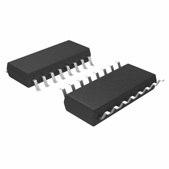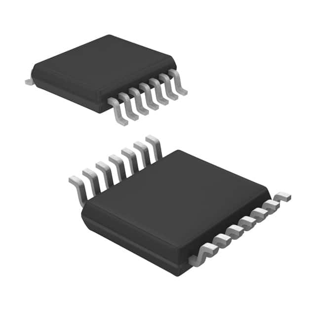
CD4027BPWRG4 Texas Instruments IC FF JK TYPE DUAL 1BIT 16TSSOP
Integraallülitused (IC-d)
Tootja number:
CD4027BPWRG4
Tootja:
Tootekategooria:
Kirjeldus:
IC FF JK TYPE DUAL 1BIT 16TSSOP
RoHs olek:
Andmetabelid:
Elementide arv :
2
Funktsioon :
Set(Preset) and Reset
Kella sagedus :
24MHz
Maksimaalne levimisviivitus @ V, Max CL :
90ns @ 15V, 50pF
Osa olek :
Active
Päästiku tüüp :
Positive Edge
Paigaldustüüp :
Surface Mount
Pakend/ümbris :
16-TSSOP (0.173", 4.40mm Width)
Pakendamine :
Tape & Reel (TR)
Pinge – toide :
3 V ~ 18 V
Praegune – vaikne (Iq) :
4µA
seeria :
4000B
Sisendvõimsus :
5pF
Töötemperatuur :
-55°C ~ 125°C (TA)
Tüüp :
JK Type
Väljundi tüüp :
Differential
Vool – väljund kõrge, madal :
6.8mA, 6.8mA
Bittide arv elemendi kohta :
1
Laos
23,473
Ühiku hind:
Võtke meiega ühendust Pakkumine
CD4027BPWRG4 Konkurentsivõimelised hinnad
ChipIcil on ainulaadne tarneallikas. Pakume oma klientidele CD4027BPWRG4 konkurentsivõimelise hinnaga. Saate nautida meie parimat teenust, ostes ChipIc CD4027BPWRG4. Parima hinna saamiseks saidil CD4027BPWRG4 võtke meiega ühendust.
Hinnapakkumise saamiseks klõpsake
CD4027BPWRG4 Iseärasused
CD4027BPWRG4 is produced by Texas Instruments, belongs to Loogika – Flip Flops.
CD4027BPWRG4 Toote üksikasjad
:
CD4027BPWRG4 – Loogika – Flip Flops disainitud puhvervõimendid ja toodetud Texas Instruments.
CD4027BPWRG4, mida pakub Texas Instruments, saab osta CHIPMLCC-st.
Siit leiate erinevaid juhtivate tootjate elektroonilisi osi rahu.
CHIPMLCC CD4027BPWRG4 on range kvaliteedikontrolliga ja nõuetele vastav kõike nõuetele.
CHIPMLCC-s näidatud fondi staatus on ainult viitamiseks.
Kui te ei leia otsitavat osa, võtke meiega ühendust lisateavet, näiteks varude arvu andmetabelis CD4027BPWRG4 (PDF), hind CD4027BPWRG4, Pinout CD4027BPWRG4, manuaal CD4027BPWRG4 Ja CD4027BPWRG4 asenduslahendus.
CD4027BPWRG4 FAQ
:
1. What is the maximum supply voltage for CD4027BPWRG4?
The maximum supply voltage for CD4027BPWRG4 is 18V.
2. What is the typical operating frequency range for CD4027BPWRG4?
The typical operating frequency range for CD4027BPWRG4 is 0 to 10MHz.
3. What is the maximum power dissipation for CD4027BPWRG4?
The maximum power dissipation for CD4027BPWRG4 is 500mW.
4. What is the minimum input voltage for a logical high level for CD4027BPWRG4?
The minimum input voltage for a logical high level for CD4027BPWRG4 is 3.15V.
5. What is the maximum propagation delay time for CD4027BPWRG4?
The maximum propagation delay time for CD4027BPWRG4 is 60ns.
6. What is the maximum quiescent current for CD4027BPWRG4?
The maximum quiescent current for CD4027BPWRG4 is 8µA.
7. What is the maximum operating temperature range for CD4027BPWRG4?
The maximum operating temperature range for CD4027BPWRG4 is -55°C to 125°C.
8. What is the pin configuration of CD4027BPWRG4?
The pin configuration of CD4027BPWRG4 consists of 16 pins, including VDD, VSS, and various input and output pins.
9. What is the recommended operating conditions for CD4027BPWRG4?
The recommended operating conditions for CD4027BPWRG4 include a supply voltage range of 3V to 15V and an operating temperature range of -55°C to 125°C.
10. What are the typical applications for CD4027BPWRG4?
CD4027BPWRG4 is commonly used in electronic switching circuits, counters, and frequency dividers due to its reliable performance and low power consumption.
CD4027BPWRG4 Seotud märksõnad
:
CD4027BPWRG4 Hind
CD4027BPWRG4 Maalimine
CD4027BPWRG4 Tihvtide pinge
Pakkumised: Kiire hinnapakkumise kontroll
Minimaalne tellimus: 1
Sisaldab "CD40" seeria tooteid