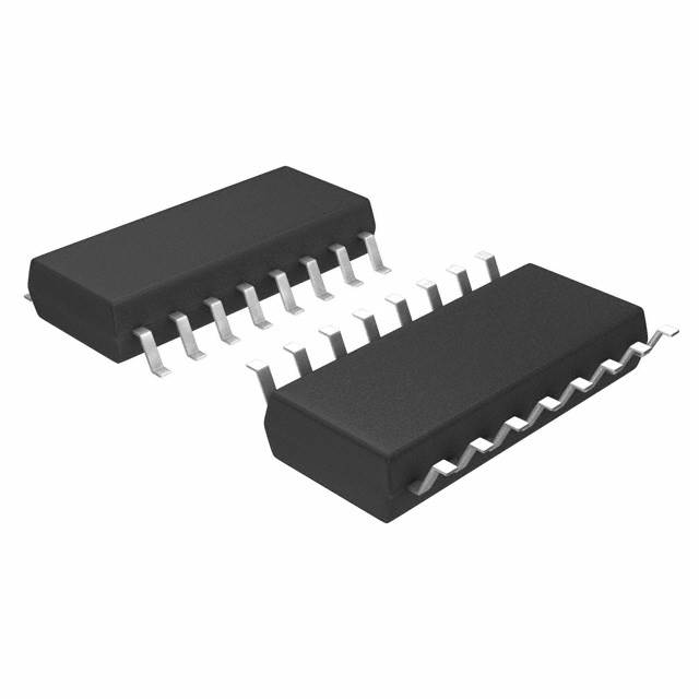
CD4011BCN ON Semiconductor IC GATE NAND 4CH 2-INP 14-DIP
Integraallülitused (IC-d)
Tootja number:
CD4011BCN
Tootja:
Tootekategooria:
Kirjeldus:
IC GATE NAND 4CH 2-INP 14-DIP
RoHs olek:
Andmetabelid:
Funktsioonid :
-
Loogika tase – kõrge :
3.5 V ~ 11 V
Loogika tase – madal :
1.5 V ~ 4 V
Loogika tüüp :
NAND Gate
Maksimaalne levimisviivitus @ V, Max CL :
70ns @ 15V, 50pF
Osa olek :
Obsolete
Paigaldustüüp :
Through Hole
Pakend/ümbris :
14-DIP (0.300", 7.62mm)
Pakendamine :
Tube
Pinge – toide :
3 V ~ 15 V
Praegune – vaikne (maksimaalne) :
1µA
seeria :
4000B
Sisendite arv :
2
Tarnija seadmepakett :
14-PDIP
Töötemperatuur :
-55°C ~ 125°C
Vool – väljund kõrge, madal :
3.4mA, 3.4mA
Vooluahelate arv :
4
Laos
19,782
Ühiku hind:
Võtke meiega ühendust Pakkumine
CD4011BCN Konkurentsivõimelised hinnad
ChipIcil on ainulaadne tarneallikas. Pakume oma klientidele CD4011BCN konkurentsivõimelise hinnaga. Saate nautida meie parimat teenust, ostes ChipIc CD4011BCN. Parima hinna saamiseks saidil CD4011BCN võtke meiega ühendust.
Hinnapakkumise saamiseks klõpsake
CD4011BCN Iseärasused
CD4011BCN is produced by ON Semiconductor, belongs to Loogika - väravad ja inverterid.
CD4011BCN Toote üksikasjad
:
CD4011BCN – Loogika - väravad ja inverterid disainitud puhvervõimendid ja toodetud ON Semiconductor.
CD4011BCN, mida pakub ON Semiconductor, saab osta CHIPMLCC-st.
Siit leiate erinevaid juhtivate tootjate elektroonilisi osi rahu.
CHIPMLCC CD4011BCN on range kvaliteedikontrolliga ja nõuetele vastav kõike nõuetele.
CHIPMLCC-s näidatud fondi staatus on ainult viitamiseks.
Kui te ei leia otsitavat osa, võtke meiega ühendust lisateavet, näiteks varude arvu andmetabelis CD4011BCN (PDF), hind CD4011BCN, Pinout CD4011BCN, manuaal CD4011BCN Ja CD4011BCN asenduslahendus.
CD4011BCN FAQ
:
1. What is the maximum supply voltage for CD4011BCN?
The maximum supply voltage for CD4011BCN is 18 volts.
2. What is the typical input current for CD4011BCN?
The typical input current for CD4011BCN is 1µA.
3. What is the maximum operating temperature range for CD4011BCN?
The maximum operating temperature range for CD4011BCN is -55°C to 125°C.
4. What is the maximum output current for CD4011BCN?
The maximum output current for CD4011BCN is ±8mA.
5. What is the typical propagation delay for CD4011BCN?
The typical propagation delay for CD4011BCN is 60ns.
6. What is the power dissipation of CD4011BCN at 25°C?
The power dissipation of CD4011BCN at 25°C is 500mW.
7. What is the recommended operating voltage for CD4011BCN?
The recommended operating voltage for CD4011BCN is 5V.
8. What is the maximum input voltage for CD4011BCN?
The maximum input voltage for CD4011BCN is VDD + 0.5V.
9. What is the typical quiescent current for CD4011BCN?
The typical quiescent current for CD4011BCN is 1µA.
10. What is the maximum frequency for CD4011BCN?
The maximum frequency for CD4011BCN is 2MHz.
CD4011BCN Seotud märksõnad
:
CD4011BCN Hind
CD4011BCN Maalimine
CD4011BCN Tihvtide pinge
Pakkumised: Kiire hinnapakkumise kontroll
Minimaalne tellimus: 1
Sisaldab "CD40" seeria tooteid