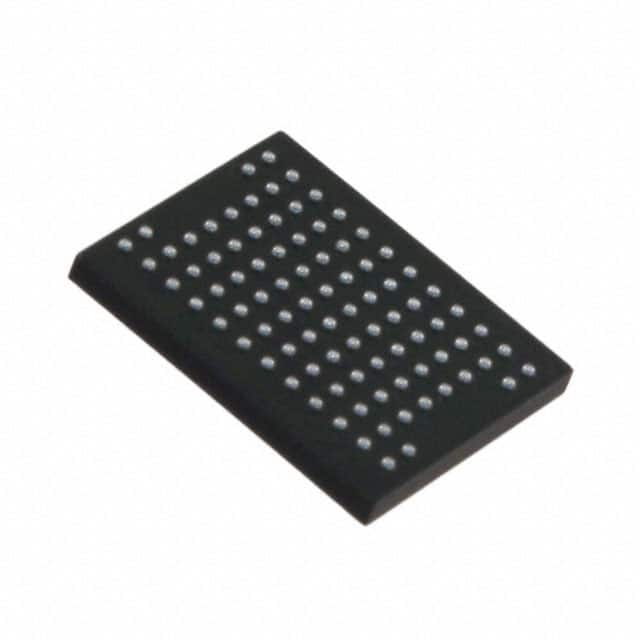
RD48F4400P0VBQE3 Micron Technology Inc. IC FLASH 512MBIT 100NS 88SCSP
Integraallülitused (IC-d)
Tootja number:
RD48F4400P0VBQE3
Tootja:
Tootekategooria:
Kirjeldus:
IC FLASH 512MBIT 100NS 88SCSP
RoHs olek:
Andmetabelid:
Juurdepääsu aeg :
100ns
Kella sagedus :
52MHz
Mälu liides :
Parallel
Mälu suurus :
512Mb (32M x 16)
Mälu tüüp :
Non-Volatile
Mälu vorming :
Flash
Osa olek :
Obsolete
Paigaldustüüp :
Surface Mount
Pakend/ümbris :
88-TFBGA, CSPBGA
Pakendamine :
Tray
Pinge – toide :
1.7 V ~ 2 V
seeria :
Axcell™
Tarnija seadmepakett :
88-SCSP (11x8)
Tehnoloogia :
FLASH - NOR
Töötemperatuur :
-40°C ~ 85°C (TC)
Tsükli aja kirjutamine – sõna, leht :
100ns
Laos
16,989
Ühiku hind:
Võtke meiega ühendust Pakkumine
RD48F4400P0VBQE3 Konkurentsivõimelised hinnad
ChipIcil on ainulaadne tarneallikas. Pakume oma klientidele RD48F4400P0VBQE3 konkurentsivõimelise hinnaga. Saate nautida meie parimat teenust, ostes ChipIc RD48F4400P0VBQE3. Parima hinna saamiseks saidil RD48F4400P0VBQE3 võtke meiega ühendust.
Hinnapakkumise saamiseks klõpsake
RD48F4400P0VBQE3 Iseärasused
RD48F4400P0VBQE3 is produced by Micron Technology Inc., belongs to Mälu.
RD48F4400P0VBQE3 Toote üksikasjad
:
RD48F4400P0VBQE3 – Mälu disainitud puhvervõimendid ja toodetud Micron Technology Inc..
RD48F4400P0VBQE3, mida pakub Micron Technology Inc., saab osta CHIPMLCC-st.
Siit leiate erinevaid juhtivate tootjate elektroonilisi osi rahu.
CHIPMLCC RD48F4400P0VBQE3 on range kvaliteedikontrolliga ja nõuetele vastav kõike nõuetele.
CHIPMLCC-s näidatud fondi staatus on ainult viitamiseks.
Kui te ei leia otsitavat osa, võtke meiega ühendust lisateavet, näiteks varude arvu andmetabelis RD48F4400P0VBQE3 (PDF), hind RD48F4400P0VBQE3, Pinout RD48F4400P0VBQE3, manuaal RD48F4400P0VBQE3 Ja RD48F4400P0VBQE3 asenduslahendus.
RD48F4400P0VBQE3 FAQ
:
1. What is the maximum operating frequency of the RD48F4400P0VBQE3 semiconductor?
The maximum operating frequency of the RD48F4400P0VBQE3 semiconductor is 100 MHz.
2. What is the typical power consumption of the RD48F4400P0VBQE3 in active mode?
The typical power consumption of the RD48F4400P0VBQE3 in active mode is 50mW.
3. Can the RD48F4400P0VBQE3 operate at extended temperature ranges?
Yes, the RD48F4400P0VBQE3 can operate at extended temperature ranges from -40°C to 85°C.
4. What is the maximum data retention period of the RD48F4400P0VBQE3?
The maximum data retention period of the RD48F4400P0VBQE3 is 20 years.
5. Does the RD48F4400P0VBQE3 support hardware data protection features?
Yes, the RD48F4400P0VBQE3 supports hardware data protection features such as block lock and OTP (one-time programmable) memory.
6. What are the available package options for the RD48F4400P0VBQE3?
The RD48F4400P0VBQE3 is available in a 48-ball VFBGA (Very Fine Pitch Ball Grid Array) package.
7. What is the erase/program cycle endurance of the RD48F4400P0VBQE3?
The erase/program cycle endurance of the RD48F4400P0VBQE3 is 100,000 cycles.
8. Can the RD48F4400P0VBQE3 be used in automotive applications?
Yes, the RD48F4400P0VBQE3 is suitable for use in automotive applications and complies with AEC-Q100 Grade 3 specifications.
9. What voltage levels does the RD48F4400P0VBQE3 support for read and write operations?
The RD48F4400P0VBQE3 supports voltage levels of 1.7V to 1.95V for read operations and 2.7V to 3.6V for write operations.
10. Is the RD48F4400P0VBQE3 compatible with standard SPI (Serial Peripheral Interface) protocols?
Yes, the RD48F4400P0VBQE3 is compatible with standard SPI protocols for easy integration into various systems.
RD48F4400P0VBQE3 Seotud märksõnad
:
RD48F4400P0VBQE3 Hind
RD48F4400P0VBQE3 Maalimine
RD48F4400P0VBQE3 Tihvtide pinge
Pakkumised: Kiire hinnapakkumise kontroll
Minimaalne tellimus: 1
Sisaldab "RD48" seeria tooteid