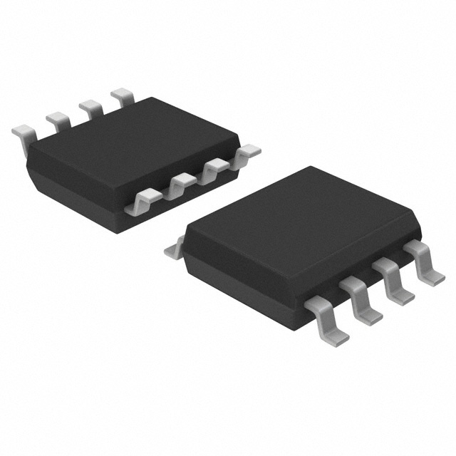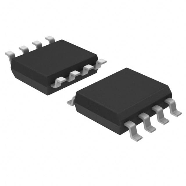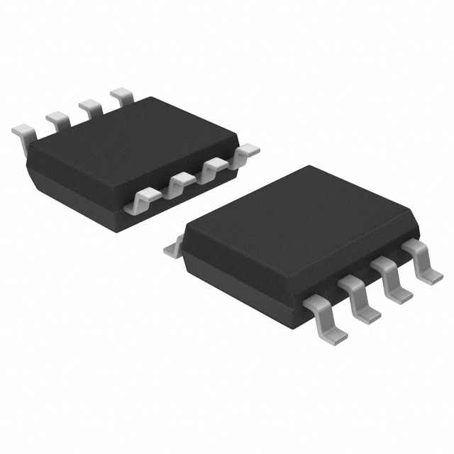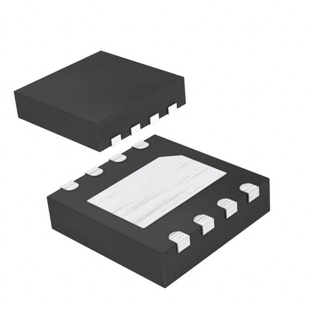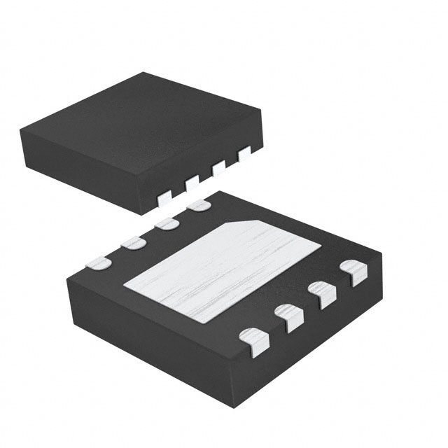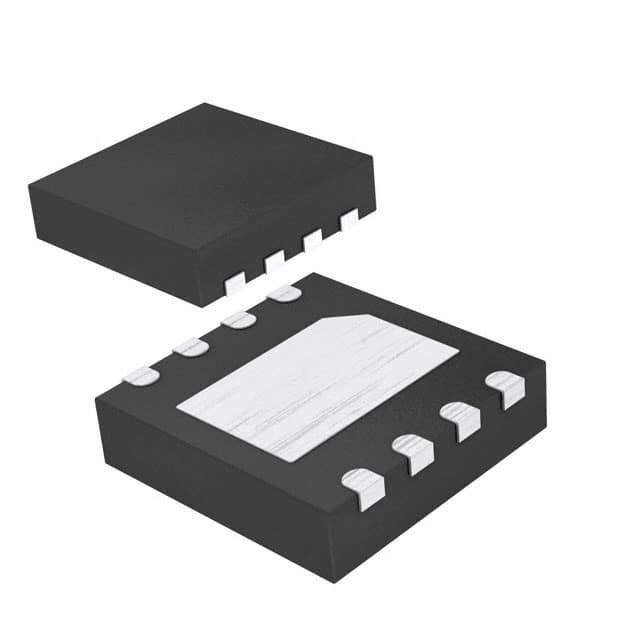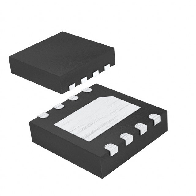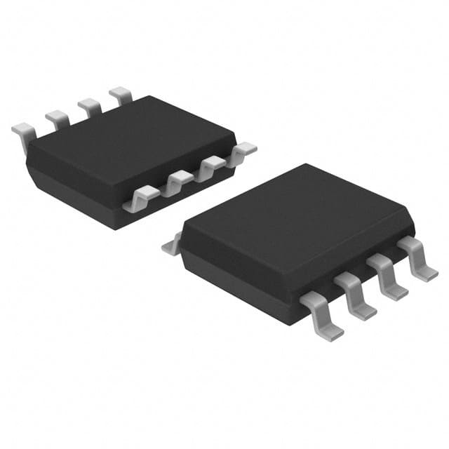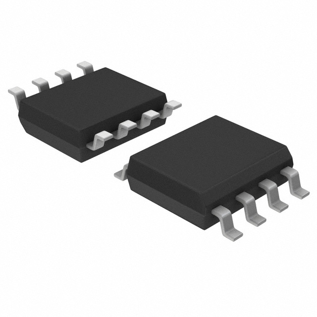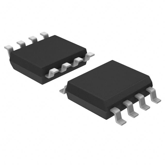

IS25WD040-JBLE ISSI, Integrated Silicon Solution Inc IC FLASH 4MBIT 80MHZ 8SOIC
Integraallülitused (IC-d)
Tootja number:
IS25WD040-JBLE
Tootekategooria:
Kirjeldus:
IC FLASH 4MBIT 80MHZ 8SOIC
RoHs olek:
 Pliivaba / RoHS-iga ühilduv
 Andmetabelid:
 IS25WD040-JBLE Andmetabelid(PDF)
Juurdepääsu aeg :
-
Kella sagedus :
80MHz
Mälu liides :
SPI
Mälu suurus :
4Mb (512K x 8)
Mälu tüüp :
Non-Volatile
Mälu vorming :
Flash
Osa olek :
Obsolete
Paigaldustüüp :
Surface Mount
Pakend/ümbris :
8-SOIC (0.209", 5.30mm Width)
Pakendamine :
Bulk
Pinge – toide :
1.65 V ~ 1.95 V
seeria :
-
Tarnija seadmepakett :
8-SOIC
Tehnoloogia :
FLASH - NOR
Töötemperatuur :
-40°C ~ 105°C (TA)
Tsükli aja kirjutamine – sõna, leht :
3ms
Laos
17,134
Ühiku hind:
Võtke meiega ühendust Pakkumine
IS25WD040-JBLE Konkurentsivõimelised hinnad
ChipIcil on ainulaadne tarneallikas. Pakume oma klientidele IS25WD040-JBLE konkurentsivõimelise hinnaga. Saate nautida meie parimat teenust, ostes ChipIc IS25WD040-JBLE. Parima hinna saamiseks saidil IS25WD040-JBLE võtke meiega ühendust.
Hinnapakkumise saamiseks klõpsake
IS25WD040-JBLE Iseärasused
IS25WD040-JBLE is produced by ISSI, Integrated Silicon Solution Inc, belongs to Mälu.
IS25WD040-JBLE Toote üksikasjad
:
IS25WD040-JBLE – Mälu disainitud puhvervõimendid ja toodetud ISSI, Integrated Silicon Solution Inc.
IS25WD040-JBLE, mida pakub ISSI, Integrated Silicon Solution Inc, saab osta CHIPMLCC-st.
Siit leiate erinevaid juhtivate tootjate elektroonilisi osi rahu.
CHIPMLCC IS25WD040-JBLE on range kvaliteedikontrolliga ja nõuetele vastav kõike nõuetele.
CHIPMLCC-s näidatud fondi staatus on ainult viitamiseks.
Kui te ei leia otsitavat osa, võtke meiega ühendust lisateavet, näiteks varude arvu andmetabelis IS25WD040-JBLE (PDF), hind IS25WD040-JBLE, Pinout IS25WD040-JBLE, manuaal IS25WD040-JBLE Ja IS25WD040-JBLE asenduslahendus.
IS25WD040-JBLE, mida pakub ISSI, Integrated Silicon Solution Inc, saab osta CHIPMLCC-st.
Siit leiate erinevaid juhtivate tootjate elektroonilisi osi rahu.
CHIPMLCC IS25WD040-JBLE on range kvaliteedikontrolliga ja nõuetele vastav kõike nõuetele.
CHIPMLCC-s näidatud fondi staatus on ainult viitamiseks.
Kui te ei leia otsitavat osa, võtke meiega ühendust lisateavet, näiteks varude arvu andmetabelis IS25WD040-JBLE (PDF), hind IS25WD040-JBLE, Pinout IS25WD040-JBLE, manuaal IS25WD040-JBLE Ja IS25WD040-JBLE asenduslahendus.
IS25WD040-JBLE FAQ
:
1. What is the maximum clock frequency of the IS25WD040-JBLE flash memory?
The maximum clock frequency of the IS25WD040-JBLE flash memory is 133 MHz.
2. What is the operating voltage range for the IS25WD040-JBLE?
The operating voltage range for the IS25WD040-JBLE is 2.7V to 3.6V.
3. Can the IS25WD040-JBLE operate in extended temperature ranges?
Yes, the IS25WD040-JBLE can operate in extended temperature ranges from -40°C to 85°C.
4. What is the typical read access time of the IS25WD040-JBLE?
The typical read access time of the IS25WD040-JBLE is 104 ns.
5. Does the IS25WD040-JBLE support software and hardware write protection?
Yes, the IS25WD040-JBLE supports both software and hardware write protection features.
6. What is the maximum data retention period of the IS25WD040-JBLE?
The maximum data retention period of the IS25WD040-JBLE is 20 years.
7. Is the IS25WD040-JBLE compatible with SPI interface?
Yes, the IS25WD040-JBLE is compatible with Serial Peripheral Interface (SPI).
8. What is the package type of the IS25WD040-JBLE?
The IS25WD040-JBLE is available in a standard 8-pin SOIC package.
9. Can the IS25WD040-JBLE be used for over-the-air (OTA) firmware updates?
Yes, the IS25WD040-JBLE can be used for over-the-air (OTA) firmware updates in IoT applications.
10. Does the IS25WD040-JBLE have built-in ECC (Error Correction Code) functionality?
Yes, the IS25WD040-JBLE has built-in ECC functionality to ensure data reliability.
The maximum clock frequency of the IS25WD040-JBLE flash memory is 133 MHz.
2. What is the operating voltage range for the IS25WD040-JBLE?
The operating voltage range for the IS25WD040-JBLE is 2.7V to 3.6V.
3. Can the IS25WD040-JBLE operate in extended temperature ranges?
Yes, the IS25WD040-JBLE can operate in extended temperature ranges from -40°C to 85°C.
4. What is the typical read access time of the IS25WD040-JBLE?
The typical read access time of the IS25WD040-JBLE is 104 ns.
5. Does the IS25WD040-JBLE support software and hardware write protection?
Yes, the IS25WD040-JBLE supports both software and hardware write protection features.
6. What is the maximum data retention period of the IS25WD040-JBLE?
The maximum data retention period of the IS25WD040-JBLE is 20 years.
7. Is the IS25WD040-JBLE compatible with SPI interface?
Yes, the IS25WD040-JBLE is compatible with Serial Peripheral Interface (SPI).
8. What is the package type of the IS25WD040-JBLE?
The IS25WD040-JBLE is available in a standard 8-pin SOIC package.
9. Can the IS25WD040-JBLE be used for over-the-air (OTA) firmware updates?
Yes, the IS25WD040-JBLE can be used for over-the-air (OTA) firmware updates in IoT applications.
10. Does the IS25WD040-JBLE have built-in ECC (Error Correction Code) functionality?
Yes, the IS25WD040-JBLE has built-in ECC functionality to ensure data reliability.
IS25WD040-JBLE Seotud märksõnad
:
IS25WD040-JBLE Hind
IS25WD040-JBLE Maalimine
IS25WD040-JBLE Tihvtide pinge
Pakkumised: Kiire hinnapakkumise kontroll
Minimaalne tellimus: 1
Sisaldab "IS25" seeria tooteid